- Software Products
- Trial Software
- CAD Translation
- Testimonials
- Overview
- Pricing
- Knowledge Base
- Contact Us -
- Languages
We are available anytime to go online with you and help you review the Unisoft software. Also the software has HELP for most menu items by hovering over the menu item for a second then click any of the videos, manual or website links.
Go to STEP 1 below to start the installation for the ProntoTEST-FIXTURE software.
This installation is for either trial users or customers that have a subscription or have purchased the software. In trial mode the software is fully functional with limits only on the size of the CAD input file and output files created. Once the software is purchased it will be activated fully. If you have a subscription or have purchased the software the email you received will detail how to fully activate the software.
Follow the instructions in Follow the instructions in STEP 1 below and the ProntoTEST-FIXTURE software will be functional and ready to program your Flying Probe ATE or "Bed Of Nails" type In-Circuit ATE.
It is advisable to print this document and follow along with the procedure below!!
IMPORTING CAD FILES: A list and samples of the CAD file formats Unisoft imports are on our website at https://www.unisoft-cim.com/importers.php.
For help with your installation call us (enable JavaScript for our phone number) or email us (enable JavaScript for our email address).
Thank you!!
For Flying Probe ATE testers:
For "Bed of Nails" type In-Circuit ATE testers:
If you have not already done so download and install the Unisoft software.
*** It is advisable to print out this document and follow along the procedure below! ***
Click or cut and paste into your browser the following link to download the software:
www.unisoft-cim.com/download/requests/view-markup/view.zipAfter the download is complete unzip VIEW.ZIP then double-click on VIEW.MSI and follow the instructions on the screen to install the software. Please accept the default path on installation, it can be changed later.
The installation is complete.
Installation troubleshooting: Go to https://www.unisoft-cim.com/installation-troubleshooting.html
If you are a trial user of the software then please proceed to the next step below. If you have a subscription or have purchased or rented the software then follow the instructions in the email you received with the license file to activate the software fully and then proceed to the next step below.
Importing the CAD file — We will be processing the sample PC Board provided.
The Unisoft ProntoVIEW-MARKUP software is used to import all types of CAD and Bill of Material (BOM) data file formats. This data is also used by the Unisoft ProntoTEST-FIXTURE software.
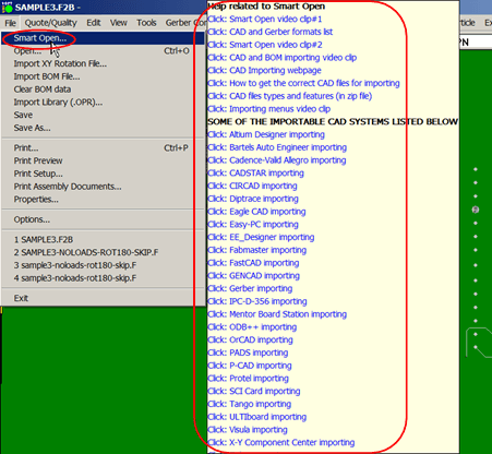
Comment: In the future to open your own CAD files you can use the SMART OPEN feature of ProntoVIEW-MARKUP which will automatically detect CAD files in a directory that can be imported into the Unisoft software. Later on to use SMART OPEN click FILE off the main menu then click SMART OPEN and point to the directory that contains your CAD files and follow the instructions to display your PC Board assembly and other files such as AutoCAD drawing files.
If you have a Flying Probe ATE then please go to STEP 5. Go to the next step if you use any other type of ATE tester such as an In-Circuit "Bed of Nails" type ATE tester.
The following steps will design the "Bed of Nails" Test Fixture.
In this step we will show how to force assign I/O pin numbers for In-Circuit "PURE PIN" ATE testers such as a Teradyne In-Circuit ATE. For multiplexed In-Circuit ATE testers this step is unnecessary because the software on the ATE tester would do the final I/O assignment.
A renumber nets example follows:
Assign power I/O connections: In the next few steps we will force assign net numbers to GND and VCC. This is a sample of how you might force assign I/O net numbers for a Pure Pin ATE Tester.
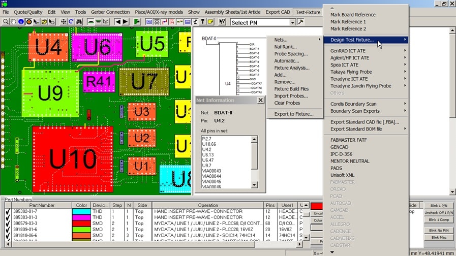
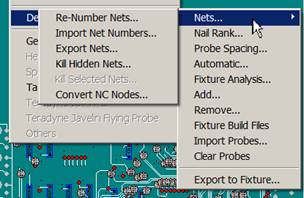
Click TEST-FIXTURE from the main top menu, then click DESIGN TEST FIXTURE then click NETS and RE-NUMBER NETS.
Fill in the VALID NET NUMBER field with MIN=0 and MAX=2000. Fill in the EXCLUDE RANGE #1 field with MIN=0 and MAX=15.
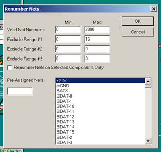
FORCED PRE-ASSIGNED NET NUMBERS (used for ground, power, etc). Use the slide bar to go down the list of Netnames until you find GND. Click GND to select and it turns blue. Next under the PRE-ASSIGNED NETS field box type in the net number you wish to assign, enter 0. Use the slide bar to go down the list of Netnames until you find VCC. Click VCC to select it and it will turn blue. Next under the PRE-ASSIGNED NETS field box type in the net number you wish to assign, enter 1.
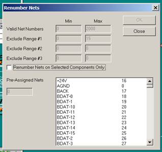
Click OK. The net numbers have now been reassigned automatically. If you use the slide bar to go down the list of Netnames you will notice that net numbers 0-15 have not been used except for the forced assignments of 0 to GND and 1 to VCC. Click CLOSE to close the window.
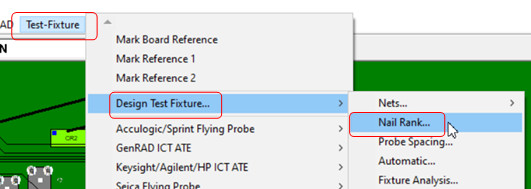
Set up Nail Rank: Click TEST-FIXTURE from the main top menu, then click DESIGN TEST FIXTURE then NAIL RANK.
The RANK NAIL CRITERIA box is displayed. Fill in the box so it appears as below. To edit the settings, click on the box to change the content. Do not press Enter to scroll between the boxes, simply click on the next box to edit it. When finished click SAVE and click OK.
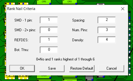
The NAIL RANK CRITERIA box above is used to set priorities for the
assigning of the test probes to each net. A “0” indicates NO, and the whole
number of “1” indicates the highest ranking followed by 2-6.
So in our
set up above we indicated using a “0” for field “SMD - 2 PIN” that we wish not
to place test probes on SMD components that are 2 pins or greater.
Also using a “0” in “BOT. THUR:” indicates that we wish not to assign any test
probes to Thru-Hole components located on the bottom of the PCB assembly ( PCBA ) because they
would have top side probing and usually it is desirable to design a test
fixture with bottom side probing only.
Then for “SMD - 1 PIN” which
stands for 1 pin SMD components which are usually test points that are
normally a preferred probing point we set that to the highest rank of “1”.
Also, in the figure above for REFDES which is an important item we have
set that to “1”. REFDES is a field define later where for example we can tell
the software to prefer the assignment of test probe edge connectors over other
components on the same net so that possible opens from edge connectors can be
tested for.
The field “SPACING” above optimizes the use of large probe
sizes such as 100mil probes and is the next most important with a "2".
Above the “NUM PINS” field optimizes probing of larger devices and is assigned
a "3".
And finally, “DENSITY” optimizes how test probes are
distributed around the PC Board to evenly allocate the forces the probes exert
and is assigned a "4".
Note: In the Rank Nail Criteria
window a field that has a 0 in it means NO or OFF and fields with a 0 are
not considered in the ranking and so multiple fields can have a 0 in them.
However whole numbers such as 1, 2, 3, 4, 5 in the fields are the actual
ranking of the execution sequence order. A field that has a whole number
ranking needs to be either higher or lower than other fields with whole
numbers in them, so you cannot repeat a whole number already used.
Set up Probe Spacing: Click TEST-FIXTURE from the main top menu, then click DESIGN TEST FIXTURE then click PROBE SPACING. The "PROBE SPACING" box is displayed and click 'RESTORE DEFAULT'.
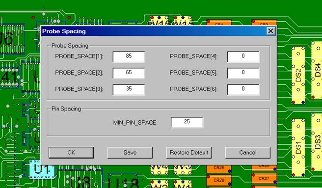
The box should appear as above 85, 65, 35 and 0 for the other PROBE_SPACE settings. The MIN_PIN_SPACE should be 25. If the settings are not as above then edit them to match. If you need to edit the settings click on the box to change the content. Do not press Enter to scroll between the boxes, simply click on the next box to edit it. When finished click SAVE and OK.
Comment: "Probe Space (1)" is normally for the 100 mil probe size. We have set it to 85 mils in the above example so if the Unisoft software selects a point to place a test probe and the closest point to that point (it's neighbor) is 85 mils or greater the software will assign a 100 mil test probe to that location. Measurements are made from center point to center point. "Probe Space (2)" is normally the 75 mil probe size and "Probe Space (3)" is typically 50 mils. As with the 100 mil probes, the software will assign a 75 mil probe if the closest point to the selected point is between 65 mils and 84 mils or a 50 mil probe if it is between 35 and 64 mils. The MIN_PIN_SPACE field is set to 25 which means that the software will not consider any point for a test probe if the center to center spacing is less then 25 mils.
Usually, the smaller size test probes 75 mils and particularly 50 mil probes are not as desirable as 100 mil test probes on your "Bed Of Nails" test fixture. Running the ProntoTEST-FIXTURE software is useful in the early stages of the PCB assembly ( PCBA ) design to detect these smaller sizes and possibly notify the CAD department so they can modify the artwork to accommodate larger test probes.
Assign the test probes automatically:
Click TEST-FIXTURE from the main top menu, then click DESIGN TEST FIXTURE then click AUTOMATIC.
The TEST FIXTURE SPECIFICATIONS box is displayed. Fill in the box
so it appears as below. To edit the settings, click on the box to change
the content. Do not press Enter to scroll between the boxes, simply click
on the next box to edit it. When finished click SAVE and click OK.
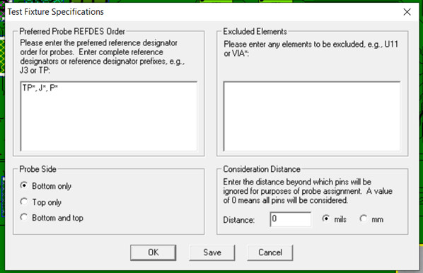
In the dialogue box "Preferred REFDES Order" above you can list the
types of component names that you may wish to place a test probe on first
in preference over other components on the same net. For example, test
points or edge connectors. To do this as a wildcard * then include the
common portion of that reference designator name to the dialog box
separated by commas. For example, TP*, J*, P* if typed in the box because
of the wildcard * would result in all components starting with either TP,
J or P being marked as preferred components. If we typed J3 in the box
then only that one component J3 would be considered preferred over other
components on the same net.
In the dialogue box "Excluded
Elements" above if any components are listed there then they will not be
assigned a test probe.
The section "Probe Side" above specifies
the type of fixture that is being designed such as bottom only, top only
or top and bottom. In the case where either “Bottom only” or “Top only” is
selected then this feature restricts where the test probes can be
assigned. For example, if “Bottom Only” is selected the result will be that
only components that have bottom side test probe access will be assigned
test probes.
The section "Consideration Distance" above is normally set to 0.
Setting something other than 0 is used in special situations, for example
where there's a cluster of predefined test points that you may wish to
assign test probes too even though they're below the minimum spacing
distance. If you wish to assign something other than 0 it is suggested
that you contact Unisoft directly for more detail.
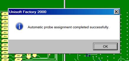
The dialog box above appears indicating that the automatic test probe assignment feature has completed and has attempted to assign one test probe to a specific point on each net.
Click OK and the dialog box closes.
This step checks if a test probe has been assigned to each net: Click TEST-FIXTURE from the main top menu, then click DESIGN TEST FIXTURE then click FIXTURE ANALYSIS. The FIXTURE ANALYSIS: NON-PROBEABLE NETS box appears similar to below showing nets that have not been assigned a test probe.
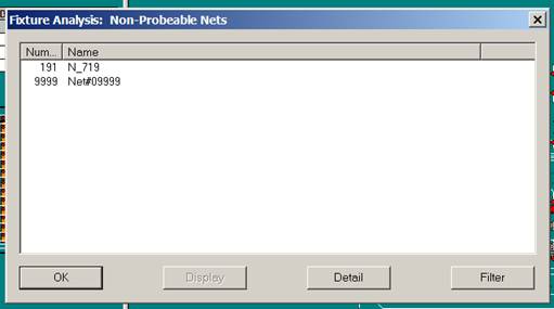
In this dialog box there are NETS that have not been assigned a Test Probe
and this is usually a serious condition because without a test probe on the
net the ATE tester can not stimulate or measure the net.
The net
number 9999 above is where any unconnected device pins are placed. Network
9999 should be ignored.
Also, an additional feature is available where
you can convert the NO CONNECTS to one pin nets automatically with the Unisoft
software. This is done by clicking TEST-FIXTURE from the main top menu, then
click DESIGN TEST FIXTURE then click NETS and CONVERT NC NODES. For our
tutorial today we will not be using this feature.
In the dialog box above click the row with the “Name” “N_719” to select the item (it turns blue), then click DETAIL. The detail about the net is now displayed.
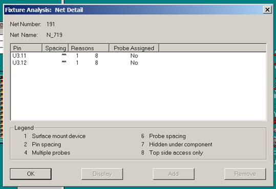
The dialog box shows the device pins U3.11 and U3.12 and to the right of these pins under REASONS there is a 1 and an 8. From the LEGEND field below, it indicates that a 1 is a SURFACE MOUNT DEVICE. So, both of these device pins are surface mount device pins and a test probe was not placed here automatically because we told the software not to probe surface mount devices earlier in the TEST FIXTURE SPECIFICATIONS dialog box. The 8 to the right of U3.11 and U3.12 from the LEGEND field indicates TOP SIDE ACCESS ONLY. Both of these device pins are on the Top Side and a test probe was not placed here automatically because we set the software not to probe Top Side device pins earlier in the TEST FIXTURE SPECIFICATIONS dialog box. This net is a problem net because there is no test probe access from the bottom side on the PCB assembly ( PCBA ) and this situation needs to be addressed.
Click OK twice to exit FIXTURE ANALYSIS.
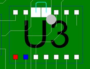
Looking closer at the problem net in question on the display, the figure below is a close-up of the top side surface mount component U3. The component pins in question are U3.11 and U3.12 and the trace is highlighted. The trace between the two pins is only on the topside. This is further confirmation of the problem the software previously identified.
Once we are satisfied with the results of the previous FIXTURE ANALYSIS step this next step creates the fixture fabrication files.
Click TEST-FIXTURE from the main top menu, then click DESIGN TEST FIXTURE then click FIXTURE BUILD FILES.
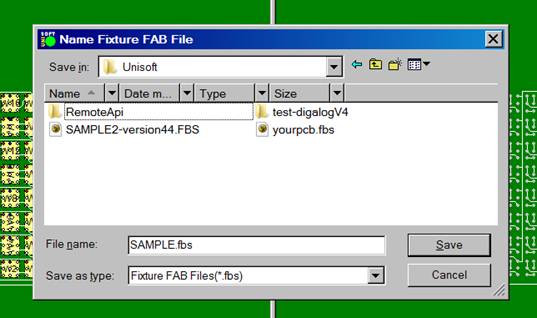
The NAME FIXTURE FAB FILE dialog box above is displayed. Click SAVE. If you are in trial mode a dialog box will appear indicating this is an unlicensed version of the software and if so, click OK to close the box.
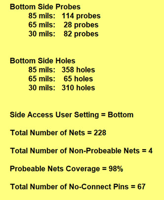
The Test Fixture fabrication and report files have now been created and are located in the directory just selected (usually c:\program files (x86)\unisoft). These files are sent to the test fixture fabrication house to build the test fixture. The files created include all the necessary drill, test probe placement and wiring files. These files help streamline and reduce errors in the fabrication process.
One of the files created, the Fixture Build Report file (.FBR), contains a listing of all the failing "no test probe access" nets. Also, it contains statistics for the total number of probes place sorted by size and also the total drill through holes for each size, no-connect pins, etc. This information is useful for designing and quoting your test fixture.
Below are details on the files just created. They are ASCII files and can be viewed with any text editor:
Sample of the .FBR report:
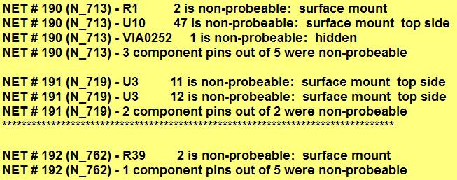
File extension .FBR is the FIXTURE BUILD REPORT FILE. The two figures above are from the .FBR file. The .FBR report file contains a net by net report. It indicates any problems that occurred when the software placed test probes and a summary report. If you search this file for ***** you will find
the net which is the net that failed previously and was not assigned a test probe
similar to the 1st figure above.
Also, it contains statistics for the total number of probes place sorted by size and also the total drill through holes for each size,
no-connect pins, etc. (2nd figure above).
Sample of the .FBS file:
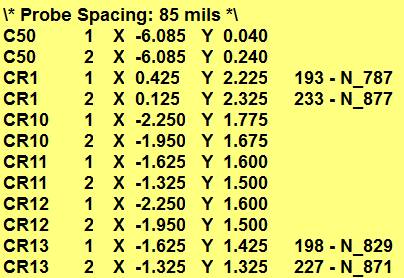
The file extension .FBS is the FULL FIXTURE SOLDER SIDE FAB FILE and is
pictured above. The .FBS file contains all the test probe locations to be
drilled and wired on the solder side of the PC Board. It also contains
all the drill through holes that will be taped over on the solder side. It
is sorted by size.
File extension .FBP is the FIXTURE FAB PROBE ONLY FILE. The .FBP file contains only the test probe locations and how they are to be drilled and wired. It is sorted by probe size.
Our clients normally send to the fixture fabrication house the three files above. Also, to help visually resolve problems they send the included UnisoftPC Board CAD Viewer & Gerber Viewer software ProntoVIEW-MARKUP.
The fixture design process is now complete. Test probes have been assigned to the best locations. Any nets that can not physically except a test probe have been detected and reported. Fixture fabrication files have been created. Below are additional optional features of the software.
In the previous step we designed and created the necessary files to build the "Bed Of Nails" Test Fixture. In this step we will create the Circuit Description file that matches the "Bed Of Nails" Test Fixture for the ATE tester.
The Unisoft software supports virtually all "Bed Of Nail" type In-Circuit testers such as Keysight/Agilent/HP 307X, GenRad, Teradyne, MDA ATE, etc. For our tutorial today we will be creating the GENRAD .CKT Circuit Description file. For details on other ATE models please call us (enable JavaScript for our phone number) or email us (enable JavaScript for our email address).
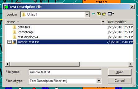
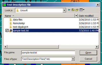
CREATING THE CIRCUIT DESCRIPTION FILE: Click TEST-FIXTURE from the main top menu, then click GENRAD ICT ATE and click GENRAD ICT ATE OUTPUT FILE . The "TEST DESCRIPTION FILE" dialog box below is now displayed. Component attributes such as Type, Value and Tolerance are imported via this dialog box. select the file SAMPLE-TEST.TST and click OPEN. Note if you do not see the file SAMPLE-TEST.TST it is located by default in the directory c:\program files (x86)\unisoft.
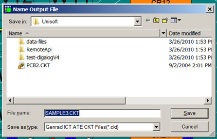
The "NAME OUTPUT FILE" dialog box below is now displayed. Type SAMPLE3.CKT in the FILE NAME field and for the SAVE IN field choose any directory you desire to save the file to. Click SAVE.
The process is now complete. A single .CKT file ready to program the GENRAD In-Circuit ATE has been created on the directory you specified. The .CKT file can be viewed with any text editor.
SAMPLE GENRAD OUTPUT .CKT
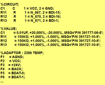
COMMENTS AND CREATING THE .TST LIBRARY FILE:
The Unisoft ProntoTEST-FIXTURE software uses a simple ASCII library to define
component part number attributes. The file extension is .TST and the image
below ".TST SAMPLE:" is a sample of what that file contains. An example of
this .TST file is SAMPLE-TEST.TST, which by default is located in the following
directory: C:\Program Files (x86)\unisoft .
The Unisoft
software looks at the .TST file and matches the part numbers of the components
on the PC Board with the part numbers in the file. Then it uses the data to
fill out information about the components on the PC Board (value, type,
tolerance, etc). That information is used to create the output files to program
the Test Equipment.
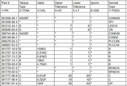
Common fields in the .TST SAMPLE file below are Part
Number(PN), Value(VAL), Upper Tolerance(UT) & Lower Tolerance(LT). The other
fields are specific for the Test equipment you are creating the output files for
and examples follow:
Genrad/Teradyne
.CKT In-Circuit ATE: The field in the ".TST. SAMPLE" figure below
labeled TGEN is the device type field for the Genrad/Teradyne In-Circuit ATE
test equipment
and some of the device types are R, C, CP, and CR.
Takaya Flying Probe: The field in the ".TST. SAMPLE" figure below
labeled TTAK is the device type field for the Takaya Flying Probe ATE test
equipment and some of the device
types are R, C, D, FET, L, IC, Q, SHORT
and C-NET for that tester.
Keysight/Agilent/HP ICT: Inserting a field labeled TKEY
would be the device type field for the Keysight/Agilent/HP ICT ATE test
equipment and some of the device types are
CONN, FETP & FETN, FUSE, L &
L(res=), J & J(type=), POT, SWITCH,
QN & QP, C, R, and D for that tester.
For more details on Keysight/Agilent/HP ICT ATE go to www.unisoft-cim.com/keysight-agilent-hp-ict-ate.html
.
Teradyne .IPL
: Inserting a field labeled TTER is the device type field for the
Teradyne .IPL ATE test equipment and some of the device types are C, R, D,
Z, IC, QN, and QP
for that tester.
The number sets the row field
for the data type. For example 1=PN indicates the part number is in row
field row below and 3=VAL indicates that the value is in the third field,
etc. This feature allows you to reorder the data fields as you prefer.
The fields in the .TST file must be separated by a TAB. To skip a field
either insert an * or leave it blank but it must contain a TAB to denote
the field.
Once part numbers are in the .TST library they can be
used over and over again.
Tip: To
quickly add new items to the .TST file customers will normally copy and
paste the appropriate rows such as the Part Number and Description from the
Bill Of Material into the TST Library to quickly enter new part numbers.
.TST SAMPLE:
Above we created the Genrad .CKT file and below are other sample test equipment and fixture setup files and Flying Probe ATE files created by the Unisoft ProntoTEST-FIXTURE software (all popular machine specific formats are supported):
*Dig U1 386EX P/N 395380-01-4;
*Cap C1 10u 20 20 f P/N 3H100M-CR-1;
*Ind L1 33u 10 10 10 f P/N 3XCTX3-32-P;
*Res R12 10k 1 1 f P/N 3XBT10-02-F;
*Devices
BATT1 1.UN002137 2.GND 5.UN002137 6.GND;
C1 1.+5VB 2.GND;
*XY
C6 1 X 2.200 Y 2.750
C6 2 X 2.200 Y 2.850
INPUTLIST, C:PCB.IPL
SH,0,1,16-1999
R,R1,"RES,P1,150k,5%",150k,5%,0,0C,C8,"CAP,C8,.1UF,20%",.1UF,20%,20%,22,0
C,C9,"CAP,C9,47UF,20%",47UF,20%,20%,22,0
D,CR3,"",0,173
D,D1,"DIODE",176,151
IC,U14,"P/N 74HCT74",74HCT74,95,96,97,98,85,84,83,82,81,92,93,99,100,101,102,103
@M SAMPLE CA9 format (Top Side)
@M Date : Thu 21.Feb.2008  22:46:19
@CE
@H -139700 -003175 -128270 -003175
C2 0.01UF 391777-06-8 * C N1 N2 @T 20 20
CR1 * 385848-05-6 * D N3 N4 @T 7 6
CR13 * 385848-05-6 * D N5 N6 @T 7 6
C3 0.01UF 391777-06-8 * C N1 N2 @T 20 20
C50 10UF 391781-01-4 * C N30 N2 @T 20 20
IP1P1 P-Auto CGND-+24V * R N39 N38 @K OP
IP2P1 P-Auto +24V-GND * R N38 N40 @K OP
P,1,00,IC,1,U1,N7,,,,,,,0258.832,0099.847,90,T,T,TC554001AFT
P,1,00,IC,2,U2,M7,,,,,,,0216.668,0099.847,90,T,T,TC554001AFT
P,1,00,IC,3,U3,M7,,,,,,,0237.750,0099.847,90,T,T,TC554001AFT
L,1,1,57,0252.882,0109.372,1
L,1,2,55,0252.882,0108.102,2
L,1,3,53,0252.882,0106.832,3
:NET
#1|S|WDT_DIS2|185
U12.5
U13.33
\* Probe Spacing: 100 mils *\
P2 1 X 3.300 Y 0.300
P2 2 X 3.200 Y 0.200
P2 3 X 3.100 Y 0.300 238 - 2402
CR2 1 X 5.275 Y 5.950
CR2 2 X 5.375 Y 5.950 378 - 1805
\* Probe Spacing: 75 mils *\
GP1 1 X 4.940 Y 5.610
GP4 1 X 2.475 Y 5.250
J1 1 X 0.700 Y 5.425 148 - 0104
J1 2 X 0.700 Y 5.504 123 - 2506
J1 3 X 0.779 Y 5.425 147 - 0005
54 - VCC C1.1 X -4.800 Y 0.320 Top Smd
149 - GND C1.2 X -4.800 Y 0.180 Top   Smd
54 - VCC C10.1 X -5.125 Y 0.720 Bottom Smd
149 - GND C10.2 X -5.125 Y 0.580 Bottom Smd
This step creates the necessary file to program your Flying Probe ATE. For our example we will be creating the output for the Takaya Flying Probe ATE machine (note all popular Flying Probe ATE machine specific formats are supported).
Note: If you have not already done so, go to STEP 2
and complete that step then come back to this Step # 5 and continue.
Mark Reference Points: For the Flying Probe ATE we need to set three reference marks on the top of the PC Board.
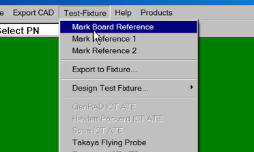
For the first reference mark click TEST-FIXTURE from the main top menu, then click MARK BOARD REFERENCE then click on the bottom of the PC Board any point in the lower left-hand side corner of the board (note for this demonstration the point you pick is not critical). The first reference point will look like the diamond in the figure below.
.
For the second reference mark click TEST-FIXTURE from the main top menu,
then click MARK REFERENCE 1 then click any point in the upper right-hand side
corner on the bottom of the PC Board. The second reference point will look
like a red diamond with the number 1 inside. For the third reference mark
click TEST-FIXTURE from the main top menu, then click MARK REFERENCE 2 then
click any point in the lower right-hand side corner on the bottom of the PC
Board. The second reference point will look like a red diamond with the
number 2 inside.
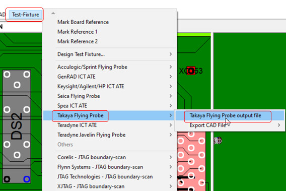
Set Takaya Specifications: Click TEST-FIXTURE from the main top menu, then click TAKAYA FLYING PROBE and click TAKAYA FLYING PROBE OUTPUT FILE.
The dialog box below “Takaya Specifications” is displayed. In the field
SIDE put a check mark in the BOTTOM SIDE box. In the dialog box
PREFERRED PROBE REFDES… type the same text as in the box
above
TP* and J1 and P* . Note each entry must be on a separate line and
it is also case sensitive so if your reference designators on the PCB assembly ( PCBA ) are
in capital letters then they must be capital letters in the boxes
PREFERRED PROBE REFDES...
For the field GROUND NET in NET
NAME select from the net name list GND (double check that you have
selected GND and not AGND or CGND). GROUND NET is used for the ground
connection for C-NET, D-NET, etc. tests. For
the field PROXIMITY
DISTANCE – MAXIMUM SHORTS RANGE (MILS): type 150 then click OK.
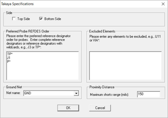
Comment 1: In the dialogue box "Preferred Probe REFDES Order…" above
you can list the types of component names that you may wish to have probed
first in preference over other components on the same net. For example, test
points or edge connectors. To do this as a wildcard * then include the common
portion of that reference designator name to the dialog box separated by
commas. For example, TP*, J*, P* if typed in the box because of the wildcard *
would result in all components starting with either TP, J or P being marked as
preferred components. If we typed J3 in the box then only that one component
J3 would be considered preferred over other components on the same net.
In the dialogue box "Excluded Elements" above if any components are listed
there then they will not be considered for probing.
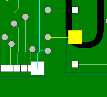
Comment 2: The
Flying Probe ATE needs to identify any shorts between nets on the PCB. In the
dialogue box above “Proximity Distance – Maximum shorts range (mils):" some of
the shorts testing can be controlled. The problem lies in that it would be
too time-consuming on a Flying Probe ATE to reposition test probes and check
each net against all other nets. So, what the Unisoft software does is set a
proximity distance limit between nets for which any two nets coming within
that distance are included in the shorts testing list and any traces outside
that distance are omitted. Since we set the field PROXIMITY DISTANCE to 150
mils any two pins on different nets coming within that distance anywhere along
their trace paths will be tested against the other trace for a potential
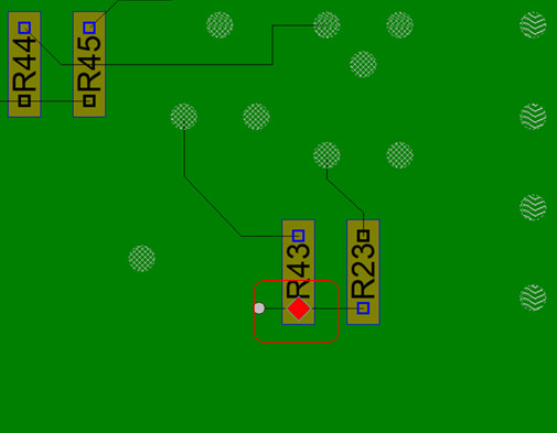
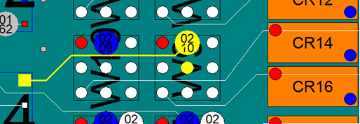
short. For example, in the figure below we see one net highlighted in blue
and the other net highlighted in yellow. In the center of the figure, we see
that these two nets come very close to each other where the two vias are
located, less than the 150 mils setting we used above, and so these two nets
would be tested against each other for a potential short. If they where
outside the 150 mils setting then those 2 nets would not be shorts tested
against each other.
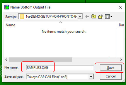
The .TST Library File: The "TEST DESCRIPTION FILE" dialog box below is now displayed. Component attributes such as Type, Value and Tolerance are imported via this dialog box. Select the file SAMPLE-TEST.TST and click OPEN. Note if you do not see the file SAMPLE-TEST.TST it is located by default in the directory c:\program files (x86)\unisoft.
The "NAME BOTTOM OUTPUT FILE" dialog box below is now displayed. Type SAMPLE.CA9 in the FILE NAME field and for the SAVE IN field choose any directory you desire to save the file to. Click SAVE.
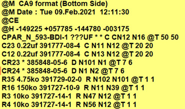
The process is now complete. Three files have been created. The first is
the .CA9 file ready to program the Takaya Flying Probe ATE and it is located
on the directory you specified and it is similar to the sample in the figure
below. The .CA9 file can be viewed with any text editor.
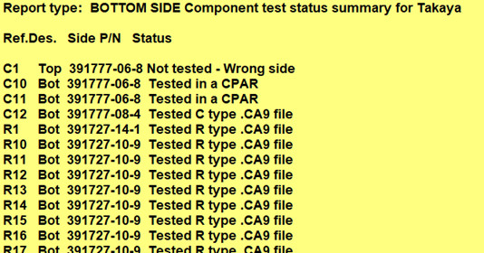
The second
file is the report file and it has the extension .TXT and it indicates the
component testing coverage details and an example is in the figure below.
The third file indicates the test probing locations and it has the
extension .FBP . Note if desired these probe locations can be mapped on the
display by clicking TEST-FIXTURE from the main menu, then click TEST-FIXTURE
DESIGN the click IMPORT PROBES and import the .FBP file.
SAMPLE TAKAYA .CA9 FLYING PROBE OUTPUT:
SAMPLE TAKAYA TEST COVERAGE REPORT FILE:
Note you may see a CPAR line or lines similar to the following in the top few lines in your Takaya .CA9 file created.
CPAR_GND-VCC ???UF * * C N1 N2 @T 50 50
If you do see one or more CPAR lines then it is necessary to edit them as outlined in the description that follows.
About CPAR:
When capacitors are in parallel they add. When the Unisoft software detects capacitors are in parallel on a PC board it creates a CPAR entry in the .CA8/.CA9 file for each pair of nodes that contain 2 or more capacitors in parallel.
The entry in the .CA8/.CA9 file will look like the following and is located at the top of the file.
CPAR_GND-VCC ???UF * * C N1 N2 @T 50 50
The N1 N2 on the line are the 2 net node trace runs that are connected to the parallel capacitors in question. In the CPAR_GND-VCC the GND-VCC portion are the 2 net names that are connected the parallel capacitors in question. The ???UF is the value of the total capacitance across those 2 nets which includes the total of all the capacitors in parallel plus any additional capacitance from IC power pins, etc. that may also be in parallel. It is necessary to enter a number in place of the ??? in the ???UF and since we can not be sure of the total capacitance we recommend you start with a reasonable number for example 5UF and then adjust it as necessary when you do the actual testing. If you do not wish a test of the capacitance across the 2 nets on any CPAR entry then remove that CPAR line from the a .CA8/.CA9 file.
The test status summary file, which is created at the same time as the Unisoft software creates the .CA9 file, will list all the capacitor reference designators that are being tested via CPAR and it looks like the following in that file.
Ref.Des. Side P/N Status

C26 Bot C26151LF Tested in a CPAR
C27 Bot C26151LF Tested in a CPAR
COMMENTS AND CREATING THE .TST LIBRARY FILE FOR TAKAYA FLYING PROBE:
The Unisoft ProntoTEST-FIXTURE software uses a simple ASCII library to
define component part number attributes. The file extension is .TST and
the image below ".TST SAMPLE:" is a sample of what that file contains. An
example of this .TST file is SAMPLE-TEST.TST, which by default is located in
the following directory: C:\Program Files (x86)\unisoft .
The Unisoft software looks at the .TST file and matches the part numbers of the components on the PC Board with the part numbers in the file. Then it uses the data to fill out information about the components on the PC Board (value, type, tolerance, etc). That information is used to create the output files to program the Test Equipment.
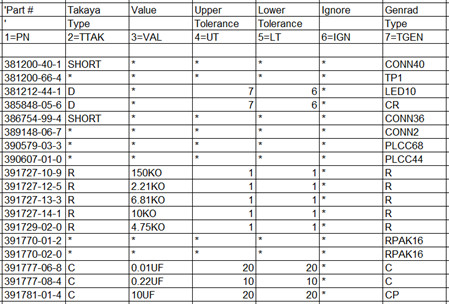
Common fields in the .TST file are Part Number (PN), Value (VAL), Upper Tolerance (UT) & Lower Tolerance (LT). The other fields are specific for the Test equipment you are creating the output files for. For example,the field below labeled TTAK is the device type field for the Takaya Flying Probe ATE test equipment and some of the device types are R, C, D, FET, L, IC, Q, SHORT and C-NET.
In the row in the .TST Sample below "1=PN 2=TTAK 3=VAL 4=UT 5=LT 6=IGN 7=TGEN" the number indicates the field for the data type. For example:
1=PN indicates the part number is in field one below.
2=TTAK indicates the 2nd field is the device type field for the Takaya Flying Probe ATE.
3=VAL indicates that the value is in the third field.
4=UT indicates that the Upper Tolerance is in the fourth field.
5=LT indicates that the Upper Tolerance is in the fifth field, etc.
The fields in the .TST file must be separated by a TAB. To skip a field
either insert an * or leave it blank but it must contain a TAB to denote
the field.
Once part numbers are in the .TST library they can be
used over and over again.
Tip: To
quickly add new items to the .TST file customers will normally copy and paste
the appropriate rows such as the Part Number and Description from the Bill Of
Material into the TST Library to quickly enter new part numbers.
Additional information on the .TST file can be found in Step 4
above in the section titled “COMMENTS AND CREATING
THE .TST LIBRARY FILE:“.
.TST SAMPLE:
Above we created the Takaya .CA9 file and below are other sample Flying
Probe ATE and other test equipment and fixture setup files created by the
Unisoft ProntoTEST-FIXTURE
software (note: All popular machine specific
formats are supported):
.ESN FILE:
P,1,00,IC,1,U1,N7,,,,,,,0258.832,0099.847,90,T,T,TC554001AFT
P,1,00,IC,2,U2,M7,,,,,,,0216.668,0099.847,90,T,T,TC554001AFT
L,1,1,57,0252.882,0109.372,1
L,1,2,55,0252.882,0108.102,2
.ASC FILE:
:NET
#1|S|WDT_DIS2|185
U12.5
U13.33
*Dig U1 386EX P/N 395380-01-4;
*Cap C1 10u 20 20 f P/N 3H100M-CR-1;
*Ind L1 33u 10 10 10 f P/N 3XCTX3-32-P;
*Res R12 10k 1 1 f P/N 3XBT10-02-F;
*Devices
BATT1 1.UN002137 2.GND 5.UN002137 6.GND;
C1 1.+5VB 2.GND;
*XY
C6 1 X 2.200 Y 2.750
C6 2 X 2.200 Y 2.850
%CIRCUIT;
C1        C         1 = VCC, 2 = GND;
R11       R         1 = N_667, 2 = BDI-15;
R12       R         1 = N_670, 2 = BDI-16;
R13       R         1 = N_671, 2 = BDI-1;
%VALUE;
C1         = 0.01UF, +20.000%, -20.000%, MSG='P/N 391777-06-8';
R11        = 150KO, +1.000%, -1.000%, MSG='P/N 391727-10-9';
R12        = 150KO, +1.000%, -1.000%, MSG='P/N 391727-10-9';
R13        = 150KO, +1.000%, -1.000%, MSG='P/N 391727-10-9';
%ADAPTOR : 2286 TEMP;
F1     = AGND;
F2     = VCC;
F3    = +24V;
F4    = BACK;
INPUTLIST, C:PCB.IPL
SH,0,1,16-1999
R,R1,"RES,P1,150k,5%",150k,5%,0,0C,C8,"CAP,C8,.1UF,20%",.1UF,20%,20%,22,0
C,C9,"CAP,C9,47UF,20%",47UF,20%,20%,22,0
D,CR3,"",0,173
D,D1,"DIODE",176,151
IC,U14,"P/N 74HCT74",74HCT74,95,96,97,98,85,84,83,82,81,92,93,99,100,101,102,103
\* Probe Spacing: 100 mils *\
P2 1 X 3.300 Y 0.300
P2 2 X 3.200 Y 0.200
CR2 1 X 5.275 Y 5.950
CR2 2 X 5.375 Y 5.950 378 - 1805
\* Probe Spacing: 75 mils *\
GP1 1 X 4.940 Y 5.610
GP4 1 X 2.475 Y 5.250
J1 1 X 0.700 Y 5.425 148 - 0104
54 - VCC C1.1 X -4.800 Y 0.320 Top Smd
149 - GND C1.2 X -4.800 Y 0.180 Top   Smd
54 - VCC C10.1 X -5.125 Y 0.720 Bottom Smd
149 - GND C10.2 X -5.125 Y 0.580 Bottom Smd
In this section we will review a few additional features of the software:
Add Test probe numbers:
From the currently open Unisoft ProntoVIEW-MARKUP software click TEST-FIXTURE from the main top menu, then click DESIGN TEST FIXTURE then click IMPORT PROBES, select the file SAMPLE.FBP displayed in the left box then click OK. A message box indicating COMPLETE is displayed. Click CLOSE. Test probe numbers and locations used on your test fixture map have just been mapped to their exact x/y positions on the included UnisoftPC Board CAD Viewer & Gerber Viewer software ProntoVIEW-MARKUP.
To find a test probe number from the main menu click EDIT then FIND and click the Probe# tab, type 210 in the box and check the "Zoom In" box then click OK. The cursor will now be over test probe #210 and the trace for that net is highlighted. If you look closely or zoom-in the there is a circle with the number 0210 indicating test probe 210. (To zoom-in either use your mouse thumb wheel or use the first icon on the left of the top tool bar then left click and hold your mouse and drag a rectangle and let go of the mouse. To zoom fully out click the 8th icon from the left on main menu "zoom to fit").
Export the netlist and x/y component pin data to a single file.
Click CAD EXPORT from the main menu, click EXPORT STANDARD CAD FILE [.FBA]. Fill out the FILE NAME and FOLDER as you wish, click SAVE. A single netlist and x/y file has been created on the directory you specified. Please view the file with any text editor. In the sample below the first field is the net number, then netname, Ref. Des., pin, X/Y and the "T" at the end on the line indicates top side and "S" indicates surface mount. Engineers find this a useful file because it lists every component and pin on the assembly.
SAMPLE .FBA:
The Unisoft software has a special feature of automatically numbering VIA's and turning them into one pin ref. des. (VIA0001.1 - VIA9999.1) and then attaches them to their net. The problem is that usually in the raw CAD data VIA's are not descript and this feature of the software is important to Test Engineers because renaming the via's to a unique name allows the test engineer to find them and add test probes to them if required.
Another feature important to Test Engineers is turning NO CONNECT PINS into one pin nets so that the test fixture can have a test probe located on this point for shorts testing, etc. A NO CONNECT PIN is a device pin that is not connected to any other pin. Typically in the CAD data these NO CONNECT PINS are not identified in the net list. The Unisoft CONVERT NC NODES feature finds these device pins and can assign net numbers to these orphan pins if you wish. To do this from the software click TEST-FIXTURE from the main top menu, then click DESIGN TEST FIXTURE then click NETS and CONVERT NC NODES. A window appears and says "YOU ARE ABOUT TO CONVERT 67 NO-CONNECT NODES". For our tutorial today we will not be using this feature so click NO. If we clicked Yes then the result would have been that each of the 69 NO CONNECT PINS would have been assigned 69 unique new net-numbers.
Export a Bill of Material (BOM).
Click CAD EXPORT from the main menu, click EXPORT STANDARD BOM FILE then click SORT BY REFERENCE DESIGNATOR and fill out the FILE NAME and select the FOLDER as you wish, click OK.

A single .BOM file similar to the above figure has been created on the directory you specified. This file can be view with any text editor.
Comment: The Unisoft software can be adjusted to import all types of BOM file formats. Instructions for importing your Bill Of Material (BOM) into the Unisoft software can be found on the Unisoft website at https://www.unisoft-cim.com/bom.htm. If you need help contact us for assistance in importing your BOM.
Create a single board database file (.F2B) with all the current PC Board and test probe information saved to an F2B file.
From the ProntoVIEW-MARKUP software, click FILE then click SAVE. The file YOURPCB.F2B has been created and is located in the directory c:\program files (x86)\unisoft under the name YOURPCB.F2B. This .F2B file is compatible with the included ProntoVIEW-MARKUP software. More information on the PCB assembly ( PCBA ) CAD Viewer & Gerber Viewer follows, also seehttps://www.unisoft-cim.com/pcbview.php.
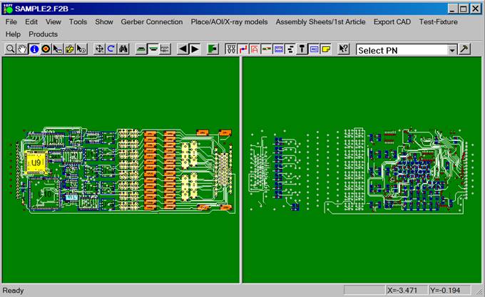
For this tutorial we will open a PC Board with additional annotation notes and steps we have previously added. From the main menu click FILE click OPEN, click CONTINUE and select the file SAMPLE3.F2B and click OPEN and click NO in the "Save Changes to sample" window. The PC Board is displayed and click CLOSE in the "Messages from importer module" window.
There are over a 100 features of the Unisoft basic software module ProntoVIEW-MARKUP below are a few example tutorials.
Note:
More detail, an overview and other links for creating assembly documents,
assigning Steps and Substeps, Coloring components, adding annotations, etc. can
be found at
https://www.unisoft-cim.com/assembly-docs-how-to-create-sample.html .
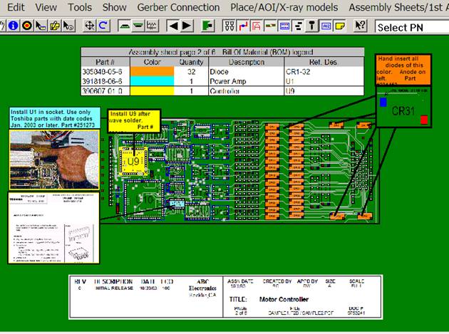
The Unisoft software allows you to quickly create matching assembly lists and assembly drawing sheets for each step in the assembly process. Part numbers are automatically assigned to the assembly step you wish (for example: Step 1 for Hand Inserts, Step 2 Chip Shooter components, etc). The part numbers are then automatically uniquely colored. If needed, overlay annotation notes can be added to each step. Next for each step matching assembly lists and assembly drawings are created. These drawings can either be printed or saved to a file (PDF Adobe, etc.) or displayed on the screen.
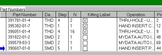
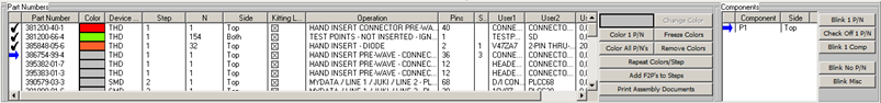
To create assembly and process sheets on the main menu click ASSEMBLY SHEETS/1st ARTICLE then click OPEN SMART COLOR OPERATIONS and a new window appears at the bottom.
The SMART COLOR window at the bottom is sortable either by Part Number, Step Number, N=number of components for that part number, Operation, number of Pins on the component, etc.
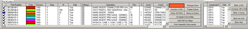
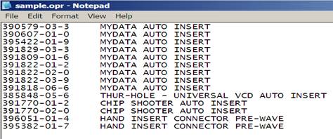
To assign an Operation to each part number from the main menu click EDIT then BOM then IMPORT LIBRARY (.OPR) and a new window will appear. In the window click on the file SAMPLE.OPR to select it then click OPEN. The result is that under the OPERATION field at the bottom of the screen each part number has been automatically assigned a operation step, for example Part Number 390579-03-3 is assigned Operation "Mydata / Mycronic AUTO INSERT".
The Operation field is optional and it is easily populated by the .OPR file which is a simple text file. The .OPR file contains the Part Number followed by a tab then the Operation text for that part number (Example: 396051-01-4 HAND INSERT SOCKET PRE-WAVE). The Operation information in the .OPR file is automatically assigned to every part number on the assembly. The SAMPLE.OPR file used in our example is located in the directory by default c:\program files (x86)\unisoft . Also the Operations can be manually entered by double clicking on the Part Number and editing the OPERATION field directly in the window provided. Then you can export and save the Operation information you have manually entered to an .OPR file by clicking EDIT then BOM then EXPORT P/N operation.
(NOTE: This exported file does not append to an existing .OPR file. It simply exports the Part Number and Operation field to a new file. Of course if you wish at that point you can manually append that file to another existing .OPR file.)
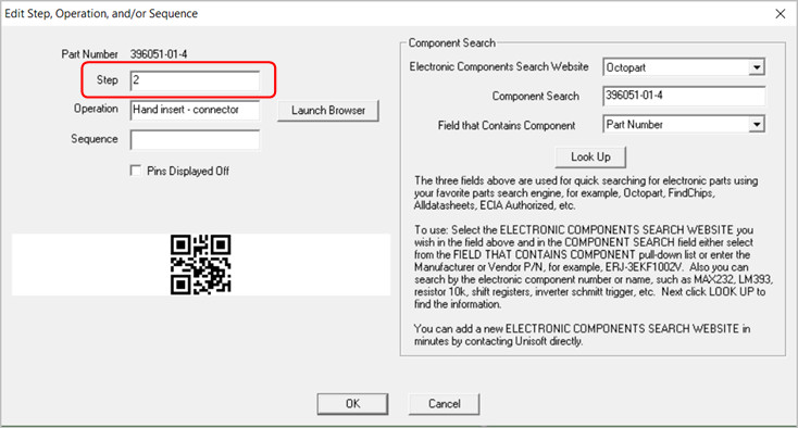
In the bottom window to the right of the PART NUMBER field you will find the STEP field. In this field you may optionally add STEP NUMBERS to part numbers in order to create separate unique steps in the PC Boards assembly process (for example: Step 1 for Hand Inserts, Step 2 Chip Shooter components, etc). To assign a STEP NUMBER to a part number at the bottom of the display double click on a part number and edit the STEP field with a step number. When the PC Board and BOM are first imported all steps are defaulted to step 1. Note that we have previously added step numbers 1 through 5 for our sample PC Board.
(Note for creating .F2P files: The .F2P files are where annotation overlays can be saved and stored for reuse. The .F2P files can contain 1 or more annotation overlay. These .F2P files can be imported for display into any PCB assembly ( PCBA ) in the Unisoft software and used simply for display or as part of the assembly process steps in the assembly documentation creation. For details on how to create .F2P files go to F2P-FILES.)
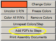
If needed overlay annotation notes can be added to each process step. To do this click ADD F2P'S TO STEPS.
The following window appears!
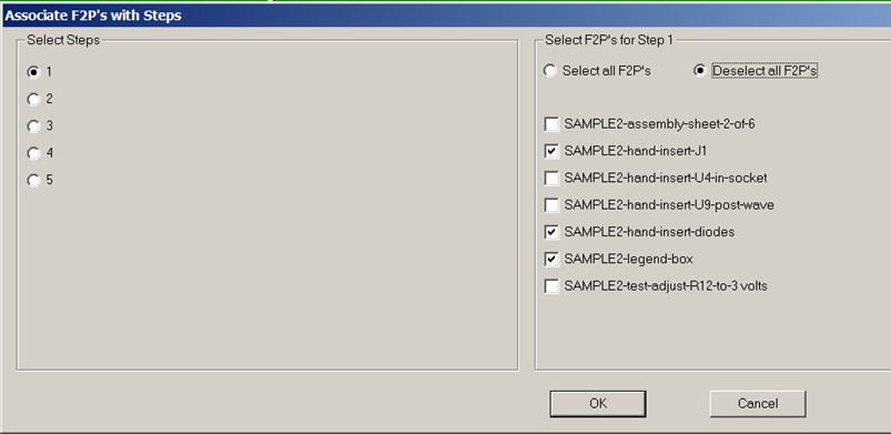
For our sample board we have previously created five process steps. Now for each one of these steps we can optionally add .F2P annotation overlay notes. In the figure above for example Step 1 is selected on the left and on the right 3 .F2P overlays boxes are checked. These four overlays will be printed on top of the PC Board display for step 1. The results would look something like the figure below. Please click on step 2 through 5 on the left side and you will see the .F2P overlays that will be printed for those steps.
(NOTE: The sample PC board we are working with already has 7 .F2P annotation overlays pre-loaded into it. It is not necessary now but in the future to add F2P Annotations to the Window above you need to Load them first. To Load Annotations from the Main menu click EDIT, click ANNOTATIONS then click LOAD ANNOTATIONS and select the .F2P file you wish to load then click OPEN.)

Note: More detail, an
overview and other links for creating assembly documents, assigning Steps and
Substeps, Coloring components, adding annotations, etc. can be found at
https://www.unisoft-cim.com/assembly-docs-how-to-create-sample.html .
In the window at the bottom click the COLOR ALL P/N's button. The "select Components" window below opens. Put check marks in this window the same as illustrated below and then click OK.
The result is that each part number and the components associated with that part number have been assigned a unique color and pattern according to the sort sequence of the part numbers in the SMART COLOR window at the bottom of the display. You also have the option to repeat the color sequence for each Step Number in the process. To do this in the window at the bottom click the REPEAT COLORS/STEP button and the colors on the PC Board will change. Note the same color will appear for different part numbers because these part numbers are in different steps. Click the UNREPEAT COLORS/STEP button again to toggle the colors to their previous state.
To freeze the colors that are currently applied to the part numbers click the FREEZE COLORS button located in the center right of the SMART COLOR window then click YES in the window that appears. Click UNFREEZE COLORS to unfreeze the colors applied to the part numbers.
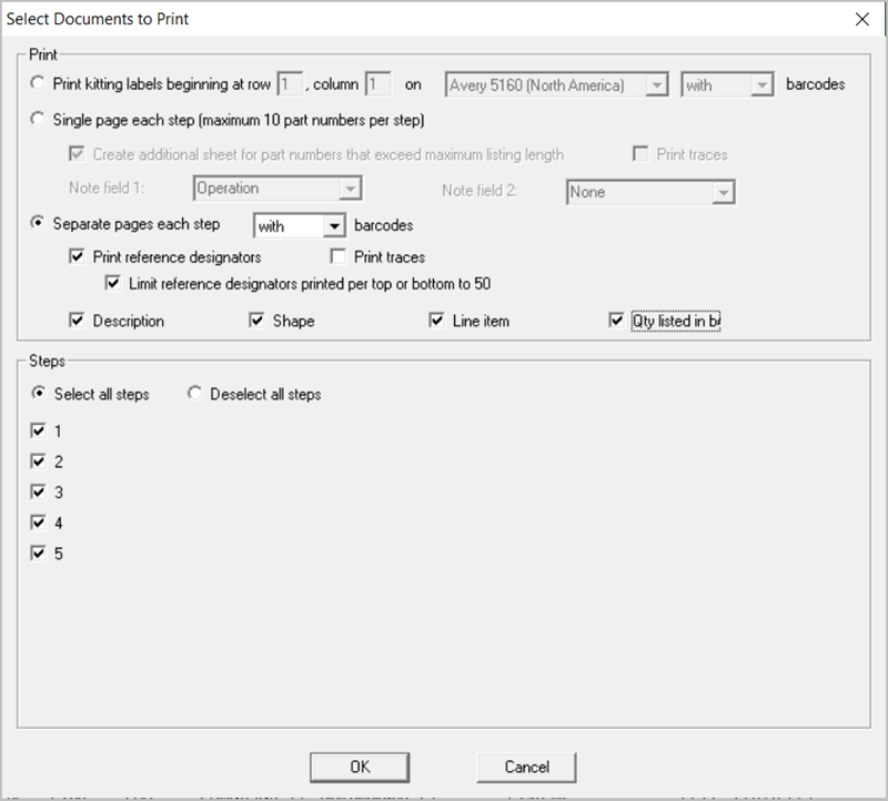
The assembly instructions for this PC Board are now complete. For this PC Board we have previously added 5 process STEPS. To Print Assembly Sheets and matching Assembly Load Lists for each process step in the window at the bottom of the display click the button PRINT ASSEMBLY DOCUMENTS.
The following window is displayed!
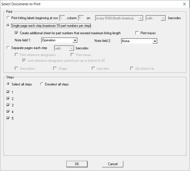
There are two options for printing Assembly Documents SINGLE PAGE EACH STEP and SEPARATE PAGES EACH STEP. The first option SINGLE PAGE EACH STEP results in a document that looks like the one below where each Step in the assembly process is printed on one sheet for each side of the PC Board assembly. Note in the figure below that the load list of the components to be inserted at that step are listed by part number at the top of the same sheet with the PC Board assembly under it and on the PC Board the components to be inserted at this step are colored with matching colors to the load list above it.
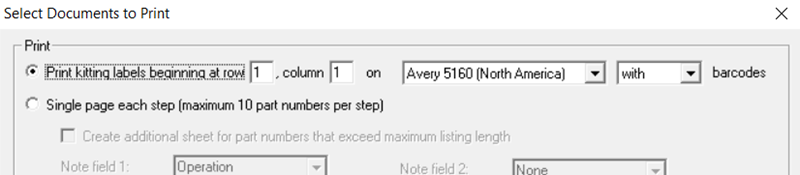
To print this drawing below in the window above under PRINT select SINGLE PAGE EACH STEP and under STEPS select select ALL STEPS. Next click OK and select the printer or PDF file you wish to print to and Click OK and the document will be printed.
Note: The check box above "Create additional sheet for part numbers that exceed maximum listing length" if checked will add an additional sheet for any part number with more components then will fit on the single sheet printout. Also NOTE FIELD 1 above is selectable to display the various data fields available and the data in that field will be displayed in the 4th column as in the figure below. NOTE FIELD 2 above can be optionally selected to be displayed and can also display the various data fields available. If NOTE FIELD 2 is selected the 4th field below will be split in half and NOTE FIELD 2 will be the 5th field.
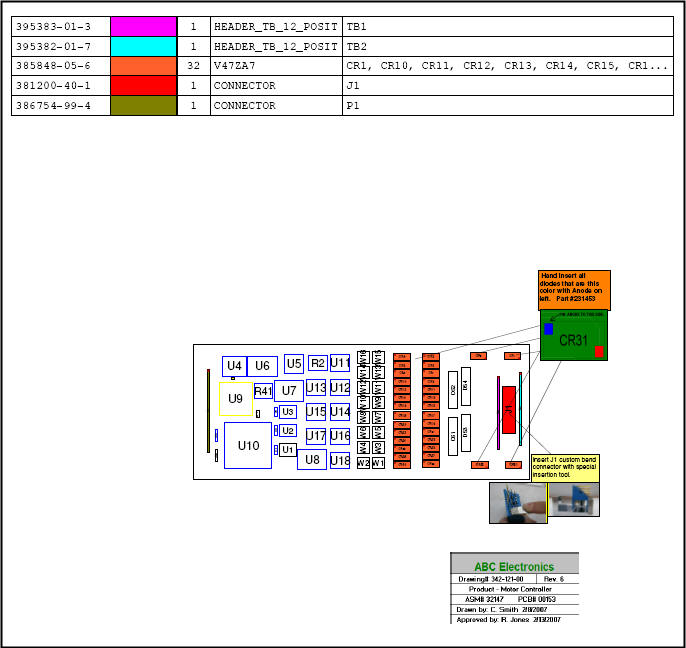
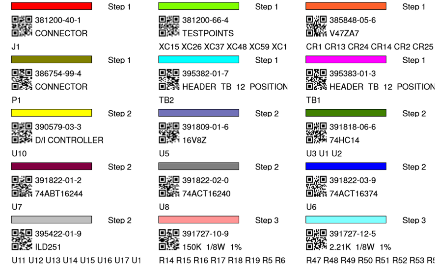
The second option for printing assembly documents is SEPARATE PAGES EACH STEP which results in a document that looks like the two figures below. The assembly drawing and the load list for each step are on separate sheets and this allows for additional space to print more information on the load list. Note in the two figures below that the load list of the components to be inserted is on its own sheet and the PC Board assembly drawing is also on its own sheet. The load list and PC Board assembly drawings have color matching components to be inserted at this step.
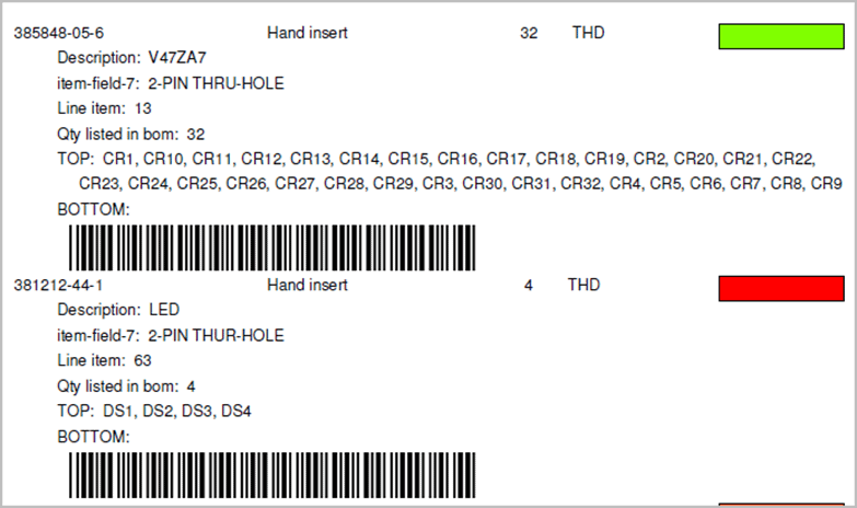
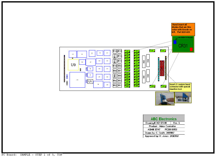
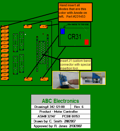
Note in the two drawings above that in the second drawing which is Assembly Sheet #1 of 5, CR1 to CR32 are colored green. Also printed are the 3 .F2P annotation overlays selected earlier for step 1 including "Hand insert all diodes that are this color", "insert J1 custom bend connector", and the legend box "ABC Electronics". In the first drawing above which is the matching Assembly Load List Sheet #1 of 5, the third item is part number 385-848-05-6 which are components CR1-CR32 and for this item we have included automatically the part number, the operation text "hand insert diodes", the quantity of 32, the device type THD, the component part number color of green, and optionally additional Bill Of Material (BOM) information of tolerance/package/description and top side reference designate listings of CR1 through CR32.
To print the drawings above at the bottom center of the main display click the button PRINT ASSEMBLY DOCUMENTS and the window below appears. Under PRINT select SEPARATE PAGES EACH STEP and then put a check mark in all the 6 boxes located under SEPARATE PAGES EACH STEP. Next under STEPS select select ALL STEPS. Then click OK and select the printer or PDF file you wish to print to and Click OK and the document will be printed.
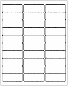
The Unisoft software allows you to quickly create Kitting Labels with barcodes for fast and accurate electronic component kitting. Quickly select the component part numbers for which you wish kitting labels created. Each label contains the part number, unique part number color, step number, p/n description, reference designator, etc. Fast and easy electronic kitting labels for kitting work orders.
Barcodes of various types can be printed on the kitting labels and shown on the display for quick kitting,
fast assembly machine feeder loading, verification, inspection, etc.: 2d-qr code, 2d-data matrix, etc.
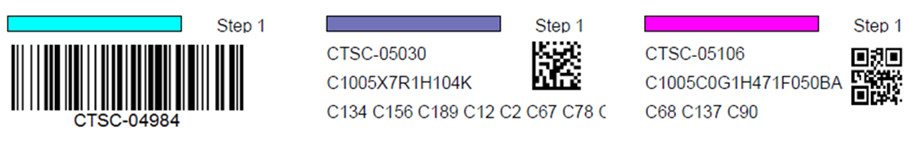
To use this feature the Smart Color window should be open at the bottom of the display and there you will see the field KITTING LABEL. By default all the thru hole component Part Numbers under the KITTING LABEL field are checked. All checked component part numbers will be included in the Kitting Label to be printed. You may add and remove checks as you wish.
To print the Kitting Labels for the checked part numbers click PRINT ASSEMBLY DOCUMENTS at the bottom middle of the display. Next select the PRINT KITTING LABELS button and click OK and OK again and if asked select the barcode type then click OK and select your printer output.
The labels created by default are standard Avery 5160 type (30 labels — 3 across & 10 down).
(Note for creating .F2P files: The .F2P files are where annotation overlays can be saved and stored for reuse. The .F2P files can contain 1 or more annotation overlay. These .F2P files can be imported for display into any PCB assembly ( PCBA ) in the Unisoft software and used simply for display or as part of the assembly process steps in the assembly documentation creation. For details on how to create .F2P files go to F2P-FILES.)
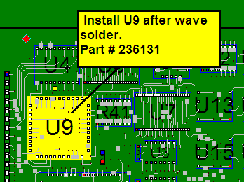
Additional text and graphics can be added to the PCB via annotation overlays and optionally saving them to .F2P files. To add annotation notes to the assembly similar to the figure below click the Annotation Tool button  on the top toolbar. Your cursor will change to
  .
.
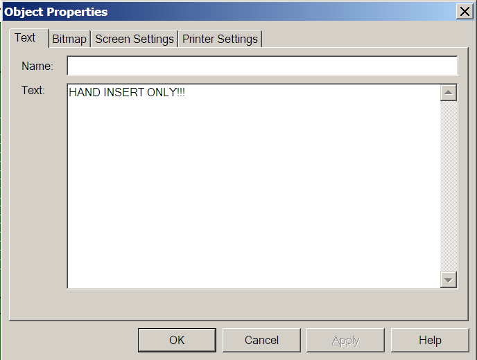
Drag a rectangle within a top or bottom view window. Release the mouse button after dragging your rectangle. The tabbed Object Properties dialog opens. This is where you can specify properties for your annotation.
Click the 'TEXT' tab or the IMAGE tab. If TEXT is selected, type your text in the Text box. The text will appear in the annotation as illustrated below. Click OK. If IMAGE is selected, import the desired image, click OK, and the image will appear in the annotation.
With the Annotation Tool selected, click the annotation you just added. For a text annotation, a shortcut menu with options will appear, as illustrated below. For an image annotation, a shortcut menu with options for modifying the image will appear.
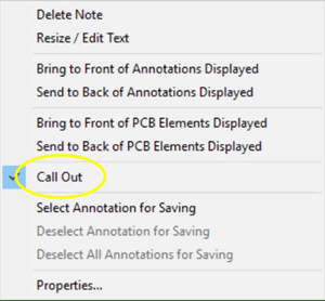
Click Call Out. A callout line appears to the right of the annotation. With the annotation cursor, click and hold the tip of the callout. Drag the callout to the desired location. While you drag, a thick line will stretch from the center of the annotation to the tip of your cursor. Note: If the tip of the callout is not in view, you may have to use the panning tool (TOOLS / PANNING TOOL) to move it into view. Release the mouse button. The callout line will move to the desired location.
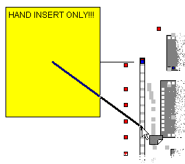
Click and drag the annotation to the desired location and note that the other end of the callout has not changed its anchor position.
Line draw tool: To create a line use the Line Draw tool by clicking the Annotation Tool button on the top toolbar until you see this icon
 with a vertical line on the left side of the yellow note then you are in the Line Draw mode. Similar to annotations, if you left-click on the line, you have the choice of deleting the line or changing its properties.
The CHOOSE F2P'S TO DISPLAY window allows you to turn on and off individual F2P annotation overlays that have been loaded.
Click the ANNOTATIONS icon  at the top of the display (it is the 3rd icon in from the right) and the "CHOOSE F2P'S TO DISPLAY" window below appears.
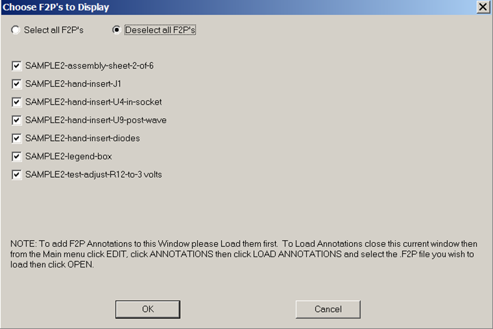
Our sample SAMPLE3.F2B file we are working with has the 7 sample .F2P Annotation overlays listed in the window above already loaded into it. These same 7 .F2B files are also on the directory by default c:\program files (x86)\unisoft. The list of the 7 F2P's are in the figure above starting with SAMPLE2-assembly-sheet-2-of-6.f2p. Feel free to load and unload them as you wish to get a feel for this feature.
NOTE: When you first start a new project no F2P annotations will appear in the window above. To add F2P Annotations to the Window above you need to Load them first. To Load Annotations from the Main menu click EDIT, click ANNOTATIONS then click LOAD ANNOTATIONS and select the .F2P file you wish to load then click OPEN.
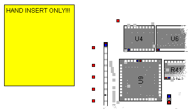
The CHOOSE F2P'S TO DISPLAY feature is also in the included viewer software so for example in the figure below an assembly person on the production floor can select the HAND INSERT overlays to help guide them with assembly.
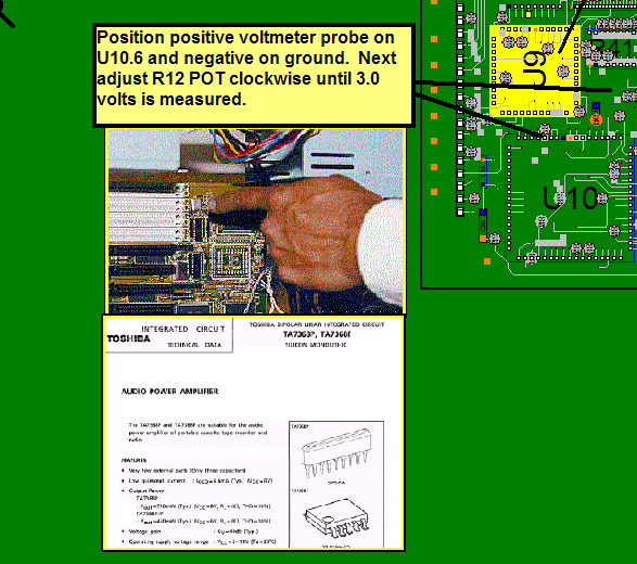
Or as in the figure below PC Board Test personnel can use the included viewer software to select the SAMPLE2-test-adjust-r12-to-3 volts.f2b overlay to guide them with a test setup procedure.
The ProntoVIEW-MARKUP included cad viewer & Gerber Viewer software can display these results for assembly personnel at their computers on your production floor or if you do not have computers they can be printed for exact assembly instructions, for example (PART NUMBER / OPERATION / NUMBER OF PARTS / COLOR).
Generally First Article Inspection is done on the first PC Boards assembled. When the assembly inspection is satisfactory at that point the PC Board can be built reliably in quantity.
After completing the tutorial above in the lower left of the SMART COLOR window at the bottom right of the display click REMOVE COLORS. In the window that opens click OK. The result is all component coloring is now cleared. Now single click the first part number displayed in the SMART COLOR window at the bottom under the "PART NUMBER" field. Then click BLINK 1 P/N located on the right side of the SMART COLOR window. This will blink those components with that part number. In real life the person doing the First Article Inspection would check each of those components for the correct part number installed. If all components with that part number are correct then they would check off that part number to indicate it is correct. Please do this now by clicking CHECK OFF 1 P/N located on the right side of the SMART COLOR window. Note a check mark has been inserted to the left of the part number indicating it has been completed and also a color has been inserted to the right of the part number in that same color has been applied to components with that part number on the displayed PC board. The inspector would continue this process for each part number until all part numbers are checked off and colored at which point that would indicate all components on the PC Board have been assembled correctly. At that point the PC Board can be built in quantity as needed.
The feature of blinking and coloring by part number or by a single component
("BLINK/COLOR 1 COMP") can also be used for other production floor operations.
For details, visit
www.unisoft-cim.com/first-article-inspection.html .
For example, for
hand-assembled components, the operator can select the part number they are
assembling by clicking that part number displayed in the SMART COLOR window
under the "PART NUMBER" field. Then, click "BLINK 1 P/N" located on the right
side of the SMART COLOR window. This will blink the components with that part
number. At this point, the person would assemble the components that are
blinking.
After all components with that part number are installed, they
would check off that part number to indicate it has been installed by clicking
"CHECK OFF 1 P/N" on the right side of the SMART COLOR window. A check mark will
then appear to the left of the part number, indicating it has been completed,
and a color will be applied to the right of the part number, which matches the
color applied to the components with that part number on the displayed PC board.
The hand assembly personnel would continue this process for each part number
they are installing by hand.
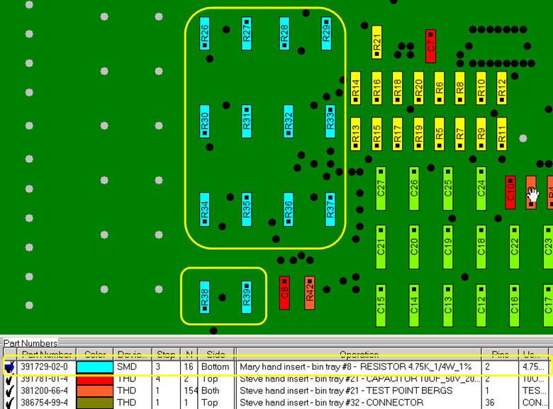
Note: Many customers that use this feature of Blinking and Coloring by part number for slide line hand assembly add additional instructions for the assembler in the Operations Field (see figure below). For example:
"Mary hand insert - bin tray #8 - RESISTOR 4.75K_1/4W_1% - p/n-391729-02-0"
Information such as this can be easily added automatically via the Operations Library or manually inserted.
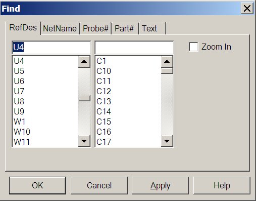
Using the FIND feature allows you to find a component or component pin. You can find a net trace or 2 net traces to identify where a short between two traces maybe. Search and find by netname or by part number. Also find by description field from the Bill Of Materials (BOM), for example find all "0.1uf capacitor". You can also find a Test Probe X/Y location and Test Probe number for your Bed Of Nails test fixture.
To open the FIND window either at the top of the display click the FIND icon  or from the main menu click EDIT then FIND. Next to search for a component type U4 in the top left field and click APPLY. The result is the cursor moves to U4 and U4 is highlighted in red. Note that APPLY finds what you are looking for and leaves the FIND window open for further finds or clicking OK closes the FIND window and locates the item you requested.
To locate a short between two traces in the FIND window in the top left field type U4.4 and in the top right field type U4.5 and click APPLY . Note as in the figure below the two traces in question are highlighted. One trace is in yellow and the other blue. A technician would then follow along the two traces and where they came closest to each other would be the most likely place to find the short.
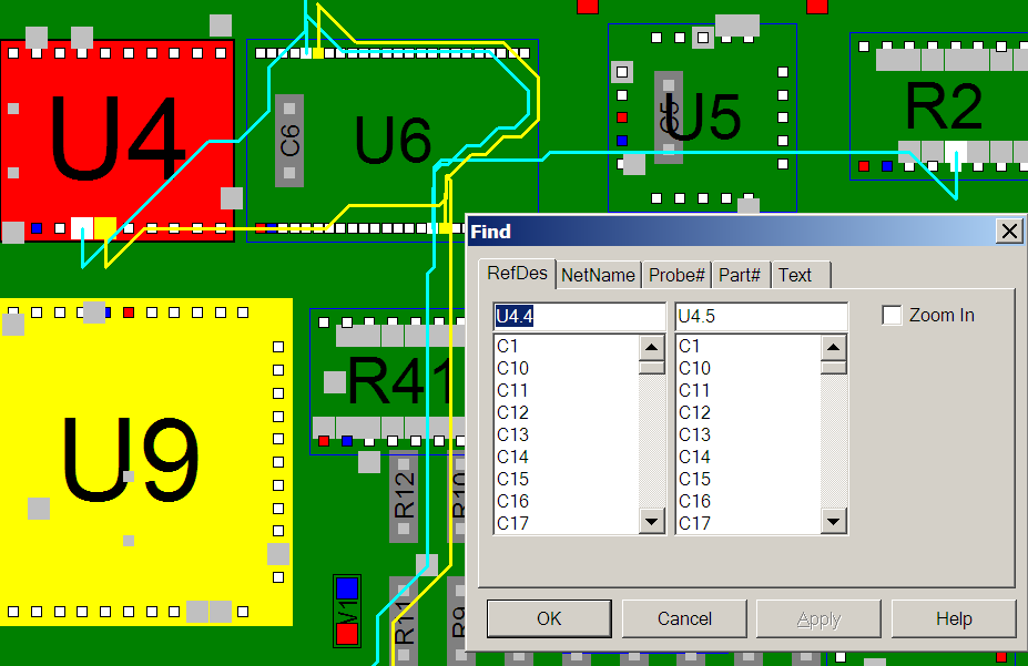
Choose any of the other tabs to experiment with the different types of search options available. Click CLOSE to close the FIND window.
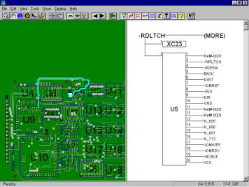
Click VIEW from the main menu then click RIGHT PANE. Click VIEW again then click SCHEMATIC. The right pane now displays "No Net selected". Click VIEW from the main menu then click LEFT PANE and select a net by either clicking the select tool (Bull's-eye icon) then clicking on a pin on the display or using the Find feature to select a net. The result is the schematic should be displayed in the right pane. The schematic view in the right pane is also an active display so by clicking any signal name or pin number on the right side on the components displayed will now navigate to that signal. You can now navigate any signal down its resultant path.
For further details on features and operations please review the manuals by clicking the "ProntoVIEW-MARKUP VIEW Manual" icon and clicking the "ProntoVIEW-MARKUP MARKUP Manual" icon in the Unisoft folder.
You will want to save your work initially or after adding annotations to your file. You can save your work as a .F2B file (complete board save) or as a .F2P overlay file (saves only annotations you have added).
To save as .F2B — On the FILE menu, click SAVE.
Note: If you want to save the file with a different name, on the FILE menu, click SAVE AS. The Save dialog box appears. Type a name in the FILE NAME box. Click OK.
An .F2B file contains all of the board information, plus the annotations. The board file is loaded first and then the annotation file is loaded on top of the board file. When you save the file, the system defaults to the original file name with a different extension. This file can be viewed by anybody using the VIEW-MARKUP software or any of the other Unisoft software modules. If you plan to send your annotated board along with the included VIEW-MARKUP program to another person, the F2B file is more convenient.
To save a .F2P overlay file — Click EDIT from the main menu, then click ANNOTATIONS and SAVE ANNOTATIONS. The Save dialog box appears. Type a name in the FILE NAME box. Click OK.
An .F2P file contains just the annotations you have added to the PC Board assembly display such as component coloring, notes and graphics. The .F2P can be viewed in conjunction with an .F2B or CAD files at a later time. If you want to develop multiple visual aids based on the same CAD file, or if you receive updated CAD files in the future, it is better to save F2P files. These files can then be loaded against the similar or updated PC Board design saving you the time of recreating the annotations. F2P's can be overlayed individually or stacked in combination.
All Pronto software modules have all the features found in the ProntoVIEW-MARKUP software and are compatible with MARKUP.EXEour included PCB assembly ( PCBA ) CAD Viewer & Gerber Viewer Software. Normally this CAD Viewer & Gerber Viewer is used throughout the plant floor or given to vendors or clients for better communications. The CAD Viewer & Gerber Viewer has over 100 features that make it the ideal ONE TOOL for the various departments of a typical electronic manufacture. Features include viewing and printing out of the display, find by Reference Designator, Part Number and more. To give the included cad viewer & Gerber Viewer to someone simply send them the MARKUP.EXE and the .F2B file for your PC Board (MARKUP.EXE is usually located in the c:\program files (x86)\unisoft directory).
To open your own cad files you can use the smart open feature which will automatically detect cad files in a directory that can be imported into the Unisoft software.
To use SMART OPEN click FILE off the main menu then click SMART OPEN and point to the directory that contains your CAD files and follow the instructions to display your PC Board assembly.
The Unisoft software imports the standard ASCII file that CAD systems create. Each CAD system has its own format. To view a variety of the latest full CAD samples please see directory c:\program files (x86)\unisoft\data-files or c:\program files (x86)\unisoft\data-files and look for the files starting with SAMPLE_. For example you will find SAMPLE_PADS.ASC which is the PADS CAD systems ASCII output file. This and the other sample CAD files can be directly imported into the Unisoft software. Simply match your file to one of the samples and your PC-BOARD can be displayed with the Unisoft software.
An API function for external control is included if you need to operate the Unisoft software from your application or equipment.
The API is contained in the file REMOTEAPI.ZIP in the directory …\unisoft where you installed the software. Please unzip this file into the …\unisoft directory. The result should be directories …\unisoft\remoteapi\rapi_test.
See the file README.TXT in the directory …\unisoft\remoteapi\rapi_test on how to use the API. Also the files API.H and RAPI_TEST.C explain the functions.
ShowCurView
ZoomCurView
OpenBoard
SetCurView
ShowCurView
ZoomCurView
Rotate
Flip
MoveCurView
ClearBom
ClearAnnotation
ImportBom
ImportAnnotation
FindComponents
FindNets
We have supplied a function tester program. You can test out the functions by running RAPI_TEST.EXE in directory RAPI_TEST. See the readme above for details.
For example, run RAPI_TEST.EXE and type HELP to get general help or type HELP FindComponents to get specific help for FindComponents. If you type FindComponents 1 U11, the 1 will zoom the display to where U11 is located and component U11 will be highlighted. If you type FindComponents 1 U11.3 U6.9 then both the component U11.3 and U6.9 pins and traces will be highlighted.
RAPI_Test — contains samples of how you can use the API via a DOS prompt.
Please note that when using the DOS command prompt test program — if you type Help at the command prompt (Enter>) you will get a list of all the API functions available to you. If you type 'help' and then the functions name (e.g., Enter>help OpenBoard) it will explain how to use that particular function. You should go through this tutorial to become familiar with the functionality of the API.
If you review the C code in the file (RAPI_Test.c) you will see how the actual DOS prompt program was written. You can write similar functions in your own code that will call up the program and launch the necessary API functions you wish.
Additional details on the Unisoft software features can be found on the Features page.
If you chose the default path on installation the software was installed to the directory c:\program files (x86)\unisoft. The executable program for the Unisoft software is MARKUP.EXE. The Icons group are installed in the PROGRAM GROUP under the Unisoft folder. Also shortcuts to the software and this quick start manual have been placed on your desktop.
Thank you for evaluating the Unisoft software. Please call us (enable JavaScript for our phone number) or email us (enable JavaScript for our email address) with any questions.